| 일 | 월 | 화 | 수 | 목 | 금 | 토 |
|---|---|---|---|---|---|---|
| 1 | 2 | 3 | 4 | |||
| 5 | 6 | 7 | 8 | 9 | 10 | 11 |
| 12 | 13 | 14 | 15 | 16 | 17 | 18 |
| 19 | 20 | 21 | 22 | 23 | 24 | 25 |
| 26 | 27 | 28 | 29 | 30 |
- FR1
- copper
- CEM1
- CMOS Image Sensor (CIS)
- FR4
- CCD sensor
- pcb
- ccd 센서란?
- 애플 반도체의 역사
- What is ccd sensor
- 히오키3480
- CEM2
- What is CCD Image sensor
- 히오키 검전기
- 에어 액츄에이터
- PCB 제조 순서
- 공압 실린더
- FMEA
- FR3
- PCB 동도금
- Copper clad laminate
- 라이프니츠 계산기
- Cis
- Image senser
- Plating
- what is CMOS sensor
- 알리 검전기
- FR2
- CMOS sensor principle
- fpcb
- Today
- Total
electronics world
What is CMOS Image sensor ? 본문
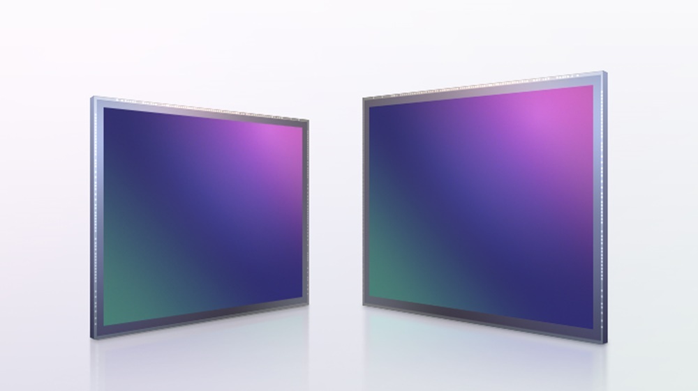
On September 2, 2021, Samsung announced the industry's first 200 million pixel mobile image sensor "Isocell HP1." What is an image sensor? Let's see how it works.
1. What is Image sensor?
The sensor used to image digital cameras and objects is called Image Sensor. Currently widely used image sensors include CCD and CMOS sensors.
When light reflected from an object touches the photodiode of the image sensor, "light" is converted into an electrical signal and transmitted to various internal devices such as serial shift registers, capacitors, and amplifiers in turn. Finally, analog-to-digital conversion takes place. The voltage signal is then converted into binary (0 and 1) values that can be processed and stored.

2. CMOS sensor principle
MOS stands for Complementary Metal Oxide Semiconductor, a mainstream semiconductor process with low-power, high-speed advantages widely used to manufacture CPU, memory, and various digital logic chips. Next, I will also post about the MOS manufacturing method, which is the basis of semiconductors. Please think that there is a CMOS in the semiconductor manufacturing process easily today.
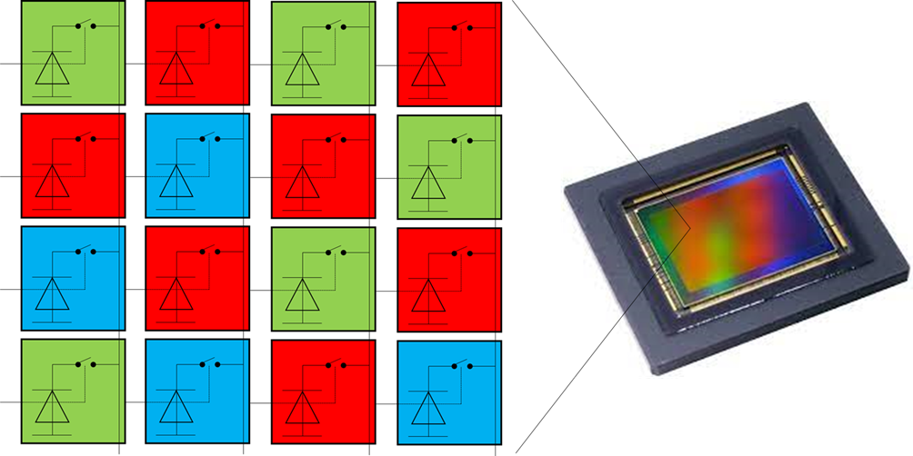
The image sensor made of CMOS semiconductor is called CMOS Image Sensor (CIS). Image sensors designed based on CMOS processes are more than 90% similar to general-purpose semiconductor processes, especially memory manufacturing processes. The CMOS image sensor switches signals of each photodiode using a CMOS switch, and each cell consists of a photodiode and a CMOS switch as shown below. (Refer to the image below) (Easy memory is a semiconductor with a lot of transistors to store 0 and 1, and CMOS is a semiconductor with a lot of photodiodes that switch from light energy to charge).
When the line drive circuit selects a row, the CMOS switch of the cell output signal is turned on, the CMOS switch of the remaining rows is not turned on, and the photoelectric signal of the line cell is transmitted to the column selection multiplexer. The column selection multiplexer consists of a series of CMOS switches and connects the sequence of signals in this row to the output to complete sequential reading of the signal column.

3. Advances in image sensors
I also have experience in developing camera modules. At that time, Sony was the unrivaled No. 1. LSI Team? (I can't remember clearly) has a strong memory of catching up with Sony, which is currently No. 1 in the world at Samsung Electronics and is expected to remain in this position for the next 10 years. Companies such as Tsinghua Uni have been chasing DRAM RAND memory technology in China, but it is difficult due to U.S. sanctions.
It is also important to increase pixels by increasing semiconductor manufacturing technology, but I personally think that AP development technology that can secure software development personnel and control sensors is more important. It is also important to secure software technology to process 200 million pixels of data accurately and without errors.

☞ 200 million pixel isocell HP1 Please refer to the link below for more information.
'New Technology' 카테고리의 다른 글
| 시스템 반도체란 무었인가?(작성중) (0) | 2022.01.21 |
|---|---|
| What is CCD Image sensor ? (0) | 2021.12.16 |
| 이미지 센서(CMOS)에 대해 알아보자 (2) | 2021.09.18 |
| 지문인식 신용카드 (0) | 2017.06.02 |
| 임배디드 인쇄회로기판 (Embedded PCB) (0) | 2017.05.29 |


